Call Now!
(408)791-2690
(408)791-2690
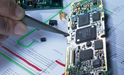
PCB Design and Layout Capabilities
With many years of experience in designing a wide range of printed circuit boards, from a simple single layer thr-hole to complex multi-layer, double-sided surface mount designs, you can count on us as your design department.

- Generate Bill of Materials / Parts Lists / Net Lists
- Convert hand-drawn schematics to digital schematic format
- Electrical Rules checks embedded net properties for layout
- Burn-In / Demo / Evaluation / Load / Socket Boards / Probe Cards
For our design, we will consider and focus the following design rules:
- Analog, Digital & Mixed Signal Designs
- Single / Double Sided & High Density
- Thr-Hole & Surface Mount Technology
- Multi-Layer and Split Planes
- Microstrip/Stripline
- Differential Pairs
- Matched Length Nets
- EMI Reduction
- Signal Integrity
- Proper Signal Return Paths
- Blind/Buried Vias
Contact us
321 E. Brokaw Road, San Jose CA 95112
Tel: (408)791-2690
Fax: (408)753-3537
Email: sales@itronixsystems.com
Send Files